I was looking into using a single VK3XDK PLL Synthesizer for both my 2.4GHz and 3.4GHz transverter systems.
ie; sharing the one PLL for both bands, with appropriate switching.
To expand on the general concept…
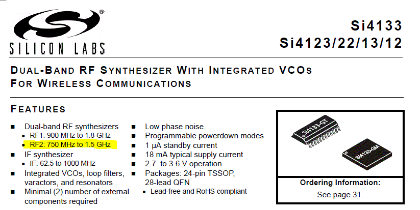
The trick is to use the Si4133’s “RF2” VCO to generate the 1484MHz, whilst the “RF1” VCO generates the 1970MHz.
The Si4133 VCO crossover is 1500MHz, so this works out well for us.
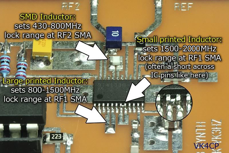
Note that, on the XDK PLL board, both of the “RF1” VCO and “RF2” VCO appear on the SMA connector labeled as “RF1” on the PCB.
Make your own cross reference to the Si4133 datasheet with caution! 😉
Most of the previous code that was out there, for some reason, used 1400MHz as the crossover, but this is easily changed.
I’m not familiar with Graham, VK3XDK’s code, as my code is a minor adaptation of what Dave, VK3HZ wrote.
It’s not important who’s code you are using, as the point of this article is to report, an XDK PLL can be used for both bands very easily.
Adapting Dave’s code was straightforward:
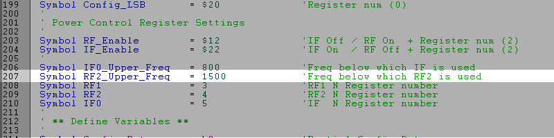
Above: This line in the VK3HZ code was changed from 1400 to 1500
My adaptation of Dave, VK3HZ’s, code:
(It’s the same code as what was attached in Graham’s topic a few weeks ago)
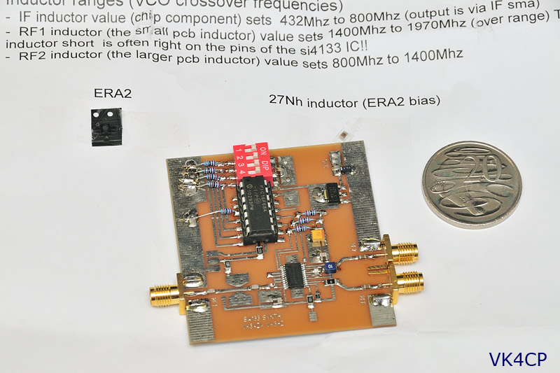
Above: The XDK PLL board showing inductors that set the center of each range
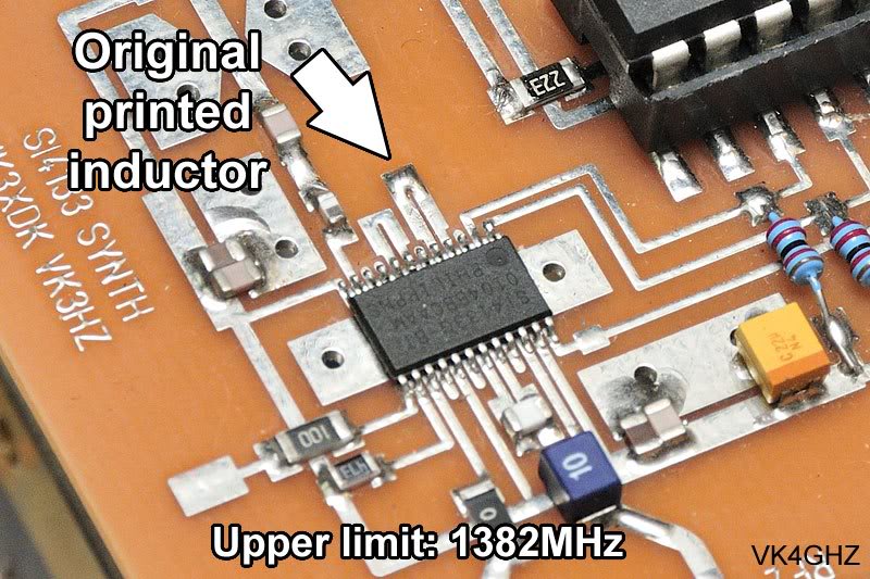
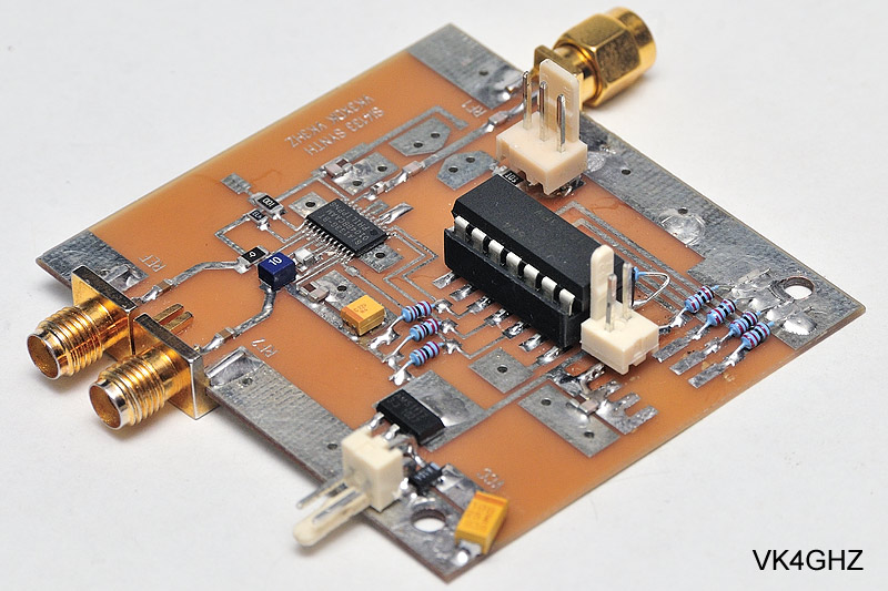
Firstly, let’s establish the current state of the XDK PLL Synthesizer board, before modifications.
It looks like this:
Not forgetting, if your PLL board has a “G” type Si4133, you will be restricted to “even MHz” output.
(No problem, this just means an IF of 433MHz for 2403MHz (1970MHz LO freq) and a 432MHz IF for 3400MHz (1484MHz LO).
On the middle range, this board was only good up to 1382MHz.
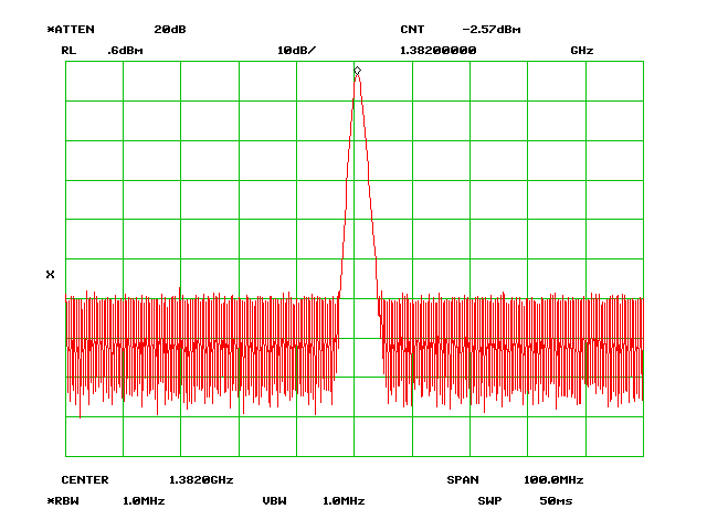
Above: Output at 1382MHz
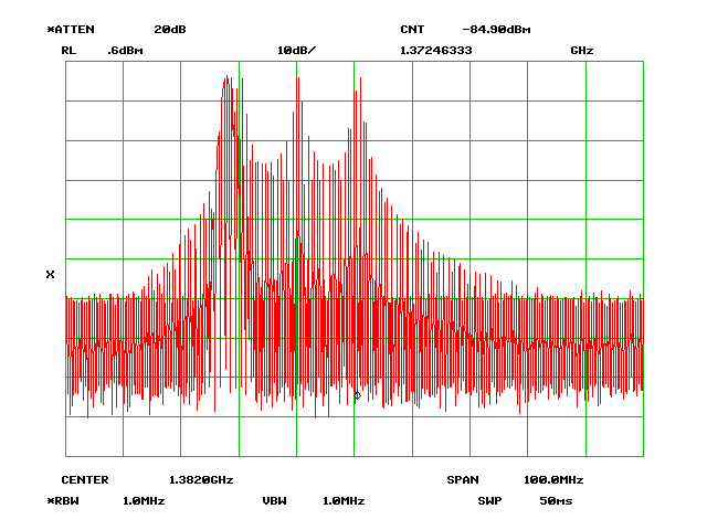
Above: Output at 1384MHz. Clearly, dirty and not locked! 1382MHz is the limit with the inductor like this.
Now, reducing the inductance, by electrically shortening the printed inductor with a solder blob, will raise the operating range.
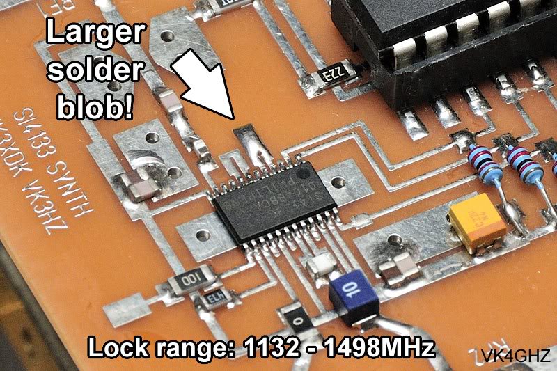
Above: Printed inductor has been reduced in value with a short that is closer to IC pins
The lock range is now an ideal 1132MHz – 1498MHz. (1498MHz being the upper limit of this VCO anyway.)
And, the other VCO, set by the solder short across pins 7 & 8 remains the same, and works fine at 1970MHz.
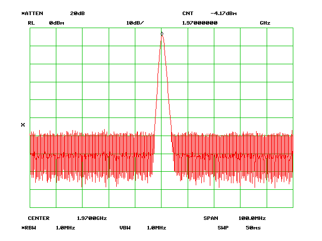
Above: Output at 1970MHz
If you don’t have access to a spectrum analyzer to check, you can replicate the larger solder short across the large printed inductor, pictured above, and have a fair degree of confidence it will “just work”.
We can then use an SMA coax relay, readily available off eBay for ~$25, or use a Minikits RF Relay kit to switch the PLL’s output to either the 2.4 or 3.4GHz transverter system.
For feeding more than two transverters, it may be better to use a low-cost 4-way splitter for Satellite TV applications.
The nominal insertion loss can be compensated for easily by adding the ERA2 MMIC and 27nH inductor that VK3XDK supplies with the PLL board.
For dual-band integration, a few hardware modifications to the VK3XDK PLL Synthesizer board have been implemented.
Above: DIP switch has been removed.
A 2-pin header HM3412 from Jaycar has been fitted across one of the DIP switch pairs, so that an external band switch can change the PLL’s operating frequency.
The legs of the header have been bent out at 90 degrees to each side, creating a surface mount part.
(I have a fetish for these headers, as I like easy connectivity, and dislike having to desolder wires to remove something!)
It doesn’t matter which pair of contacts you use, just keep in mind the corresponding PICAXE frequency table symbol addresses you will need to edit.
When the switch contacts are open, the pull down resistors will mean symbol freq00 is used, generating 1970 MHz for the 2.4 GHz system.
In this case, the external switch is across the MSB, (most significant bit) so the second frequency is symbol freq08, and the PLL will generate 1484 MHz for the 3.4 GHz system.
ie; 1484 MHz x 2 = 2968 MHz, for a 432 MHz IF
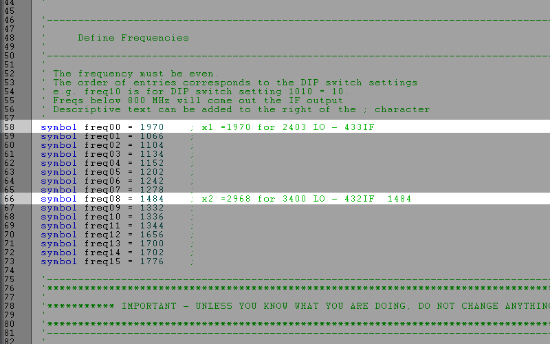
Above: Only freq00 and freq08 are of interest in this 2.4/3.4 transverter PLL.
Next, the PCB launcher SMA (f) connector was removed, and a male connector fitted in it’s place.
It’s a long story, but male launcher type SMAs for standard 1.6mm thick PCBs seem hard to find.
This male SMA connector is from RF Supplier, $1.50 each. 😀
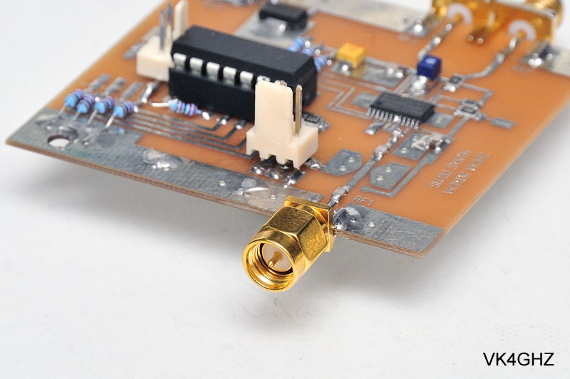
Above: SMA (m) connector fitted
Being soldered at five points, the original SMA (f) jack can be awkward to remove, but with a little care, isn’t that difficult.
The way best way (?) is to remove enough solder from the four main GND mounting tabs, and bend them, fatiguing them so they break off.
It then becomes much easier to pull straight off, whilst desoldering the centre pin.
I was trying to remove this jack so that it could be reused elsewhere, but gave up on that idea, in favor of looking after the PCB.
This then feeds an EME144 2.6 GHz RF Relay kit from Mini-Kits, which screws straight on.
I purchased the PCB and relay only, as I already had a number of SMA (f) PCB launcher jacks on hand.
The weight of the RF Relay Kit is almost nothing, and can be supported quite happily by the SMA connection.
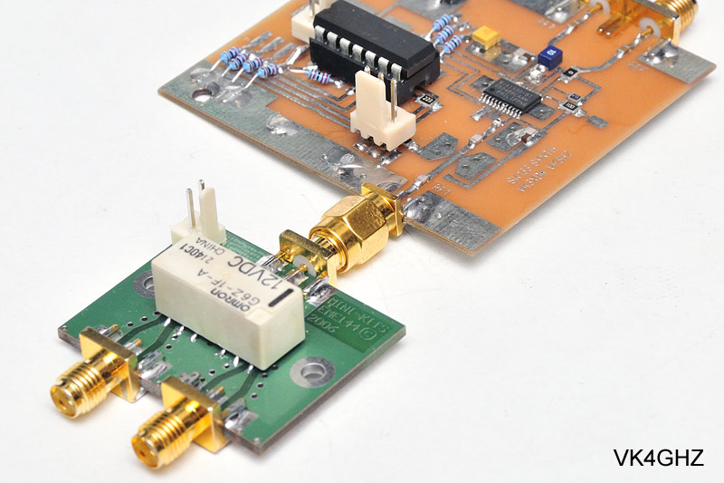
Above: EME 144 RF relay kit. Standard PCB launcher (f) jacks are used here on all ports.
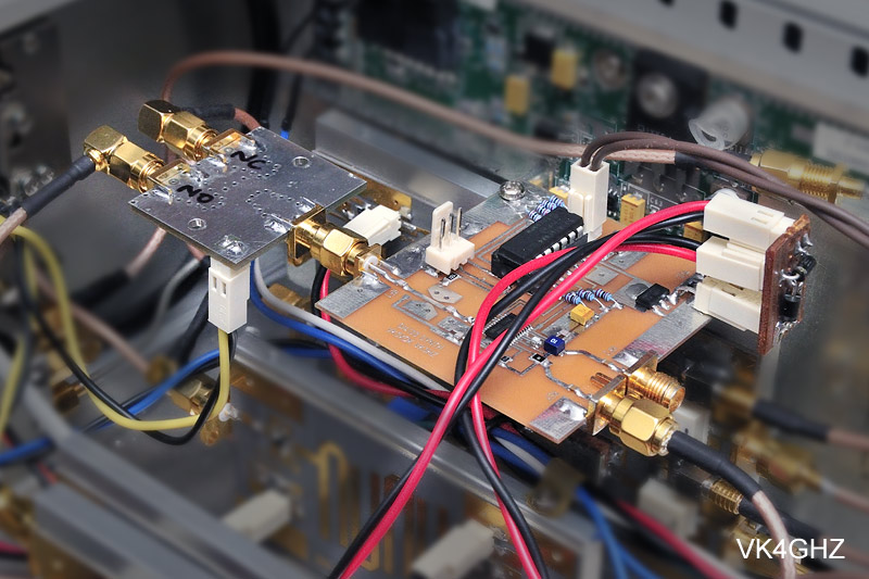
The PLL/RF Relay unit are then re-installed inside the transverter, and in this case, the relay board is orientated to best suit the cabling.
Above: Installed inside the dual-band transverter
As only one transverter system is powered up at any one time, +8V power for this PLL board comes in via a diode from each sequencer board, seen on the dual-header adapter made on a small piece of Veroboard.
(If you have a common +8V supply for all systems, you will obviously not need an arrangement like this)
The +12V to activate the EME144 relay comes the 3.4 GHz sequencer board, as this dual-band system operates on 2.4 GHz by default, unless switched across to 3.4 GHz.
This +12V control feed also switches the IF RF relay, so that the FT-817 IF rig switches from the 2.4 system, across to the 3.4 system.
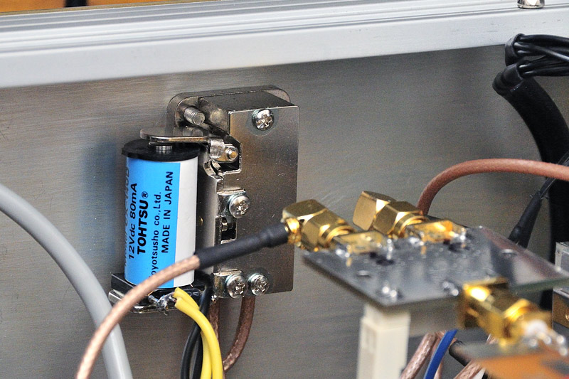
Above: Tohtsu CX-140D RF Relay from Henry Radio’s eBay store. Switches the IF rig to either the 2.4 or 3.4 systems.
😀