Hi to All !
have some difficulties to understand this schematic :
http://ok1ike.c-a-v.com/soubory/tipy/1300mc1.gif
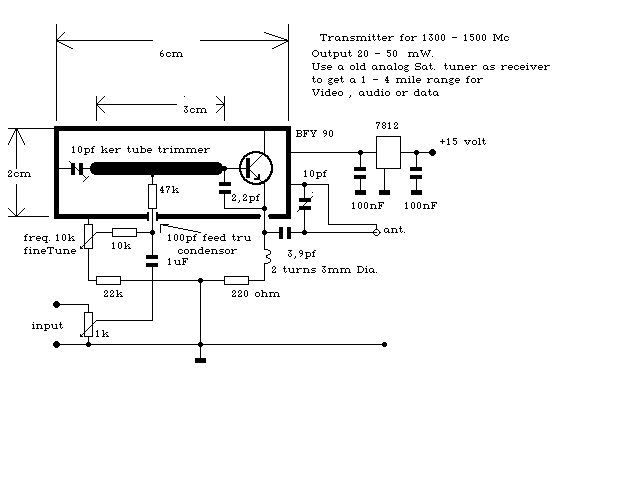
seems that the transistor is connect to sort of a shield that is on the "+" bus, also the ground of the antenna is also on the "+" (?)
the "box "that contains the transistor and a matching impedance must have specific dimensions (6cm X 3 X 2)...
the schematic is also found elsewhere without any comments.
Thank you
Patrick M.
Difficulties understanding this shematic
Re: Difficulties understanding this shematic
Hi Patrick,
Whilst I have no specific knowledge of this particular oscillator project, I'd try:
1. Make the box out of some un-etched PCB material, soldered all the way along the edges. Its easy to solder and drill.
2. I'd try 6cm x 2cm x 2cm as the box dimensions. You'll therefore need 4 pieces of 6 x 2cm and 2 pieces of 2 x 2cm PCB material to make the box.
3. Use a piece of stiff (thick) wire 3cm long for the inductor (L) in the base circuit, which runs from the 10pF tube trimmer to the base of the BFY90
4. Instead of referencing the cold side of the output connector to the "box" (which is +12v as you have noted) instead just use the circuit's ground. From an RF perspective, it's the same thing due to the 100nF bypass cap.
Good luck - I hope it works for you.
Cheers,
Ralph VK3LL
Re: Difficulties understanding this shematic
Hi Patrick
The 100n capacitor serves as a bypass for the voltage regulator. It has a too high value for the oscillator RF frequencies involved as it will be inductive at these frequencies. A smaller value ceramic in parallel, say around 100 to 470pF, should be added.
73s
Igor
VK6ZFG
Igor
VK6ZFG
Re: Difficulties understanding this shematic
Thanks VK6ZFG & VK3LL !
I think i will try to breadboard this circuit just for the fun , considering yours observations.
73 de FO4MM
I think i will try to breadboard this circuit just for the fun , considering yours observations.
73 de FO4MM
Re: Difficulties understanding this shematic
Hi Patrick
On giving the circuit some further thought (base on presence of feed through capacitor) I think that the PCB may be double sided with the inside +ve and the outside gnd/-ve. The double sided PCB acting as a bypass capacitor at RF but then the circuit does not quite make sense as the top end of the 10k would need to go to the +ve.
73s
Igor
VK6ZFG
Igor
VK6ZFG
Re: Difficulties understanding this shematic
Thank you very much for your note, Igor.
Bests regards
Patrick
Bests regards
Patrick